
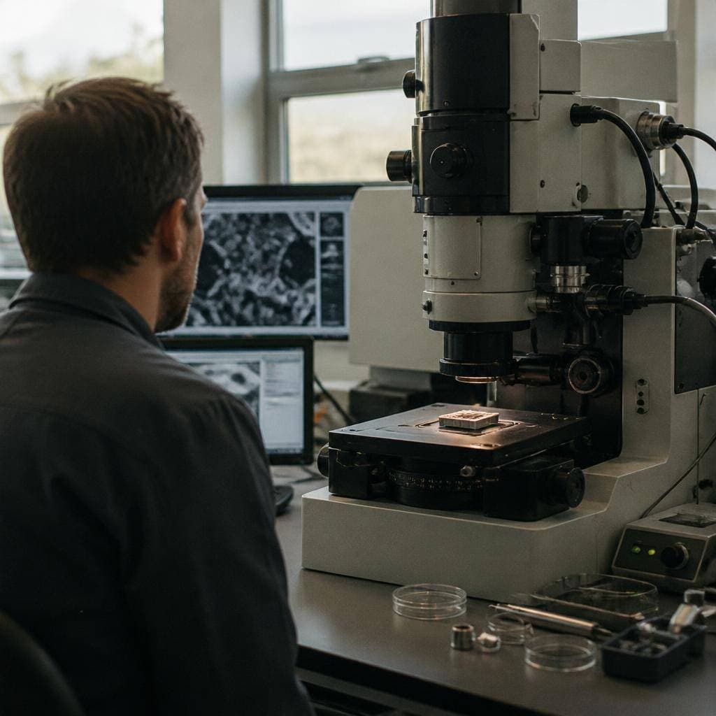
Effective product lifecycle management (PLM) demands precise material characterization and failure investigation to ensure superior product quality and durability. One critical tool in achieving this level of control is scanning electron microscopy analysis. This technique provides in-depth surface imaging and compositional data that supports informed decision-making across product development, manufacturing, and quality assurance processes.
Role of Advanced Microscopy in Product Development
In the initial stages of product design and material selection, microscopic evaluation of surface morphology and microstructure is essential. Scanning electron microscopy offers magnifications and resolution beyond traditional optical microscopes, revealing nanoscale features and potential defects that could influence performance or manufacturability.
Manufacturers leverage this insight to:
- Identify material heterogeneity that affects mechanical or chemical properties
- Analyze surface treatments and coatings to verify uniformity and adhesion
- Assess microstructural changes caused by processing conditions such as heat treatment or machining
Integration of Scanning Electron Microscopy in Failure Analysis
Throughout a product’s operational life, different failure modes can develop due to environmental stress, material fatigue, or manufacturing flaws. Understanding the root causes requires a detailed examination of fracture surfaces, corrosion patterns, or wear debris. Scanning electron microscopy excels in revealing microstructural evidence that guides corrective actions and design improvements.
Typical applications include:
- Fractography to determine crack initiation points and propagation
- Corrosion product characterization for environmental compatibility assessment
- Contaminant and foreign particle analysis to trace manufacturing anomalies
Enhancing Quality Control with High-Resolution Imaging
In mass production environments, consistent quality control is vital. Scanning electron microscopy analysis facilitates precise inspection protocols that detect sub-micron defects invisible to conventional testing methods. This capability reduces waste, rework, and warranty claims by ensuring conformance to design specifications.
Key benefits include:
- Verification of component dimensional tolerances and surface finish
- Early detection of microcracks or inclusions before assembly
- Process validation for novel manufacturing techniques such as additive manufacturing
Criteria for Selecting Scanning Electron Microscopy Services in PLM
Choosing an appropriate provider for this analytical technique involves assessing several aspects:
- Technical capability: Availability of advanced detectors (e.g., EDS for elemental analysis) and sample preparation expertise
- Turnaround time and reporting quality: Timely and detailed interpretation of results aligned with product development schedules
- Experience in relevant industries: Knowledge of sector-specific materials and failure modes
- Integration with complementary analytical tools: Access to FTIR, EDX, or XRD can provide a comprehensive characterization database
Collaborating with a service provider that understands the nuances of product lifecycle management ensures that scanning electron microscopy analysis contributes effectively to product optimization and problem resolution. A reliable laboratory offering tailored scanning electron microscopy analysis can deliver actionable insights aligned with business objectives.
Limitations and Practical Considerations
While the technique yields rich surface detail and compositional data, it has practical constraints. Sample size and preparation requirements may limit its application to certain components. Additionally, interpretation of micrographs demands specialized expertise to avoid mischaracterization of features or artifacts.
Understanding these factors allows companies to integrate scanning electron microscopy analysis appropriately within the broader PLM framework, ensuring resource efficiency and maximal information gain.
| Aspect | Considerations |
|---|---|
| Resolution | Nanometer-scale detail enabling detection of critical microdefects |
| Sample Preparation | Requires clean, conductive surfaces; may involve coating with conductive materials |
| Analysis Time | From hours to days depending on complexity and complementary tests |
| Output | High-resolution images, elemental maps, and quantitative data |
Applying scanning electron microscopy analysis within product lifecycle management presents a powerful method to detect and address material and process challenges early and throughout product use. By integrating this level of analysis, businesses enable informed decisions that extend product viability and maintain competitive quality standards.
Tags: scanning electron microscopy analysis